
Printed Circuit Board (PCB) today are extremely cheap to buy in Chinese manufacturing houses, shipping can be expensive to a certain degree, depending on how long you are willing to wait. Many argue that home made PCBs are obsolete. Personally, I strongly disagree, as there is still no way to make design iterations using a fabrication house half as fast! I can fabricate a PCB in just one hour, try to compare that with a 2-5 days lead time and 3-14 days shipment time.
Sure, the quality of home made PCBs is lesser:
- They are typically fabricated without a solder mask, making trace bridging while soldering more frequent.
- They are limited to two layers.
- Vias are a pain in the ass, as the holes going through are not metalized and require an insertion of a conductor for every single one of them.
- It is impossible to make traces as small as 3.5 mil (advertised by JLBPCB). The smallest I was able to make is 8 mil.
If the prototype can tolerate these limitations, the design can be accelerated and completed in a matter of days and the feeling of having something that looks so professional made at home is highly satisfactory!
I have made many prototyping using home made PCBs and was always frustrated by doing the process manually using very cumbersome techniques to heat and stir the etchant. For this reason I have designed and built an etching station that makes the process very fast and automatic! You can read about the full fabrication process in another post in the blog, in this post I will concentrate on the etching station design.
Etching station
In this section I will describe in detail every part of the etching station, in the hope that it will inspire others to pursue making one of their own, taking my design as a whole or just a part of it. I will begin with describing the chemistry, and continue with the mechanical design. The source files for the mechanical design, electrical design and code can all be downloaded here.
Note, that the 3D printed parts are all made of PETG. The plastic has shown good resilience to the etchant, though, if you own Polypropylene filament, it may be a better choice for this application.

Chemistry
The etchant I use is copper-chloride (Cu2Cl), it produces very little waste and can be renewed by solely adding Hydrochloric (HCl) acid to the solution. You can read more on the subject on this website.
The reaction of the etchant is the following:
CuCl2 {aq} + Cu {s} → 2CuCl {aq}
As copper is being etched into the solution, the CuCl2 concentration lowers and the CuCl concentration is rises, slowing down the reaction, and eventually stops it completely. Luckily, the etchant can be regenerated by adding oxygen to the solution:
2HCl {aq} + 2CuCl {aq} + O {aq} → 2CuCl2 {aq} + H2O{aq}
This can be done by either adding hydrogen per-oxide, or, by bubbling air into the solution.
At some point white CuCl crystals should appear in the solution and will not disappear even when the solution is added with oxygen. This is an indication that the solution HCl. This occurs as chlorine (Cl2) evaporates from the solution and as regenerating the solution after each etching consumes more of the acid.
To create the copper-chloride etchant I used 30% HCl mixed with 3% hydrogen peroxide (H2O2) and copper wire. When the solution became dark green, I removed the leftover copper filtered out solid contaminant.
Keep in mind that the solution fumes out chlorine gas (it’s toxic!), especially when it is heated. Moreover, chlorine gas is heavier than air, and may stay below the window level if the room is not ventilated with wind or a fan.
Mechanical Design
The etching station is made of the following components:
- A Bath containing the etching solution.
- Heating element alongside a temperature sensor – heats up the solution and boosts the etching rate.
- Stirring magnet – speeds up the reaction by stirring the solution, constantly renewing the solution in contact with the copper surface.
- Bubble stone – regenerates the etchant by bubbling air through the solution.
- Exhaust – evacuates the toxic fumes outside (and allows etching even in a closed room).
Bath
The bath itself is an airtight food container, it has a glass bottom and a plastic top. The glass is ideal for its high resistance to chemicals and heat, and the plastic cover is ideal for easy drilling to add feed-throughs for the different components of the etching bath.
Temperature control
The heating element is a PCB with traces zigzagging across the plate. It is has a resistance of 7Ω, designed to deliver 50W at 19V of a laptop power adapter. The heating element is coupled to the glass bottom via thermal paste, and is glued with RTV around its perimiter. Similar heating elements can easily be sourced in online stores, they are very popular in desktop 3D printers, the resistance may vary from board to board, but the power delivery can be adjusted using an additional step up/down module.
The temperature sensor is a ds18b20 soldered to a band of three wires. It is protected from the etching solution with a silicon tube (aquarium airline tube) which was sealed with RTV glue on one end . The control loop is operated by a micro-controller (uC) that turns on and off according to aset-point defined by the user.


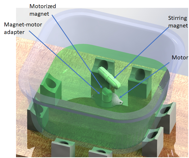
Stirrer
The stirrer is a PTFE (Teflon) coated magnet, magnetically couple to a motor mounted Neodymium magnet (with the help of a 3D printed mount) below the bath. The motor is a DC type and is speed controlled via PWM, as speed should be adjusted so the motor does not move too fast that the stirring magnet fails to follow.
Etchant oxidation
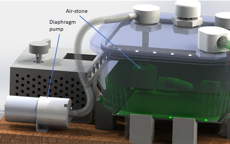
To revert the solution to it’s oxidative state the etchant is pumped with air in the form of small bubbles generated by the air stone. The air stone is pressured by a small diaphragm pump, and PWM controlled by the uC. It may be worth noting that once in a while the air-stone becomes clogged (I’m unsure why), but it can be undone simply by soaking it in hydrogen peroxide (or laundry bleach).
Exhaust
As we boost the etching rate using temperatures of ~50°C the evaporation rate of chlorine gas increases greatly. To remove the fumes, a pump sucks the air inside the enclosed bath, and evacuates it out of the room. The pump I use is a Venturi pump I designed and reported on in another blog post I published. The Venturi pump is powered by the air flow generated by a diaphragm pump and the air from inside the bath is sucked out and continues out through the remaining port of the pump.
As the fumes are sucked out, fresh air enters through a venting port (via the small holes). When the bath is non-operational, the venting port should be shut by screwing in the cap.
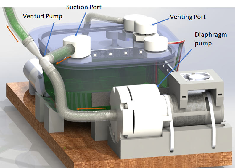
In case your are wondering, the diaphragm pump is cooled by a small fan as it heats up quite a lot. cooling it will surely increase its service.
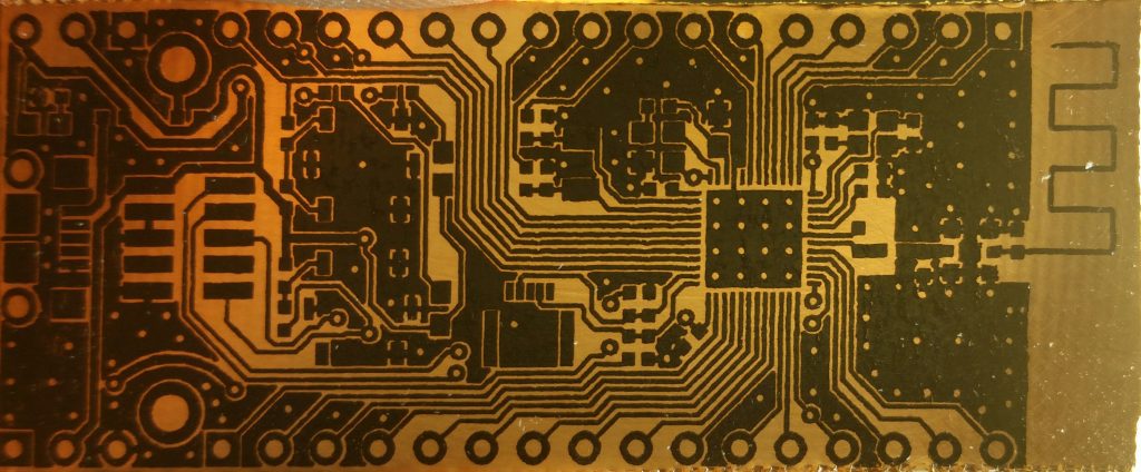
Electrical design
The device is operated using an ATMEGA328au μC. It measures the temperature inside the etching solution and controls the stirrer motor, heater and pumps using power MOSFET. The device is controlled via a simple user interface implemented with a small TFT screen (128 x 64) and a rotary encoder (EC11).
Two step down converters are installed to produce 5V and 12V rails. The first is used to power the μC and stirrer motor, the second operates the pumps and cooling fans. The two step down converters are powered by a 18/19V generic laptop power adapter (>60 watt). The heating bed is powered directly by the power adapter, though it could be nice to make a third rail in the future to adjust the voltage for different heating elements with different resistances.
The enclosure of the control board is cooled by a fan together with venting holes on the other side, forcing air to flow through.
The device can be programmed with a USB-to-Serial using the four male headers (GND,RST,RX,TX). Also, the device has a serial port for communication over Bluetooth, but no interface has been implemented up until now.


Operation
The software inside the μC is quite simple, it applies a bang-bang temperature control over the etching solution, a count-down timer for setting the etching time, and a UI for the user to interact with the configurations.
Operation modes
The device has 4 different operations modes:
- Running – All outputs are on, this is when the etching is being done.
- Purging – Only the exhaust pump is turned on. Purging mode is activated whenever the device exits Running mode, and stops after a predefined number of minutes.
- Oxidizing – The bubble pump is on (along with the exhaust). This mode is used to regenerate the solution.
- Stopped – All outputs are off.
Countdown timer
As a safety feature, the user must set the etching period before starting the device. When the time reaches zero, the device enters purging mode, after-which, it shuts down completely. To initialize the timer, simply set the “Minutes” menu to the amount of time needed to etch the board, and the click on the “Status” menu to start counting down, and see how the menu item changes from “Stopped” to “Running”.
Settings
The settings are separated into 3 submenus:
- Power Menu – Sets the output devices as enabled or disabled.
- PWM Menu – Sets the Duty Cycle of the different outputs in values of 0-255, to control the output power from 0-100%.
- Temp Menu – Sets the working temperature setpoint of the etching bath, and sets the offset value (hysteresis) of the control loop.
All of the settings are saved to the EEPROM every time they are modified by the user, and are retained even when the device is not powered.
Etching station at work
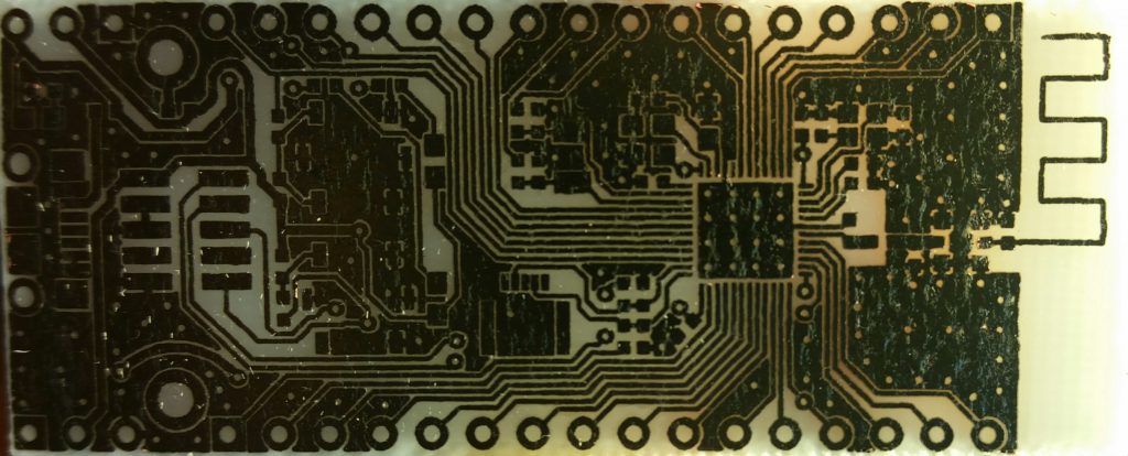
To show off the capabilities of the etching station, I decided to fabricate a relatively high detail PCB. I chose the Nordic nRF52832 module layout, shipped with the EAGLE 9 software as a sample layout. The traces in this model are 0.2mm wide (<8 mil), and the clearance of the ground plane is only 0.15m (6 mil), quite challenging I would say!
I began by transferring the printed toner onto the copper board
And soaked it into the etching bath, which was preheated to 50C°
This video is a fast forward recording of the etching process recorded by an endoscope installed inside the bath. The image quality isn’t great, where vapors condensed on the lens and distorted the image of the PCB. Also, the etching time was long (50 minutes), as I had to lower the stirring speed substantially to have a good view of the board. Typically, the etching process would amount for less than 10 minutes.
I removed the PCB from he solution and rinsed it with water
And wiped the toner off the board with acetone and paper
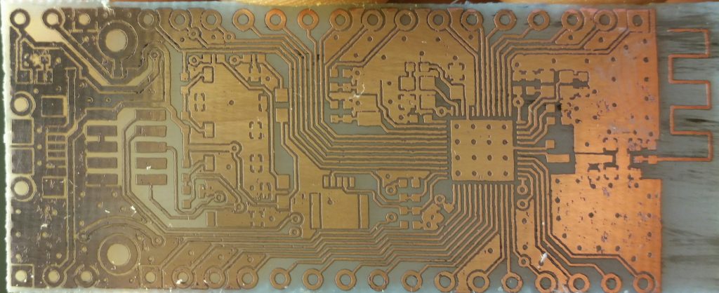
and recorded another picture with back-light to get a good image of the flaws
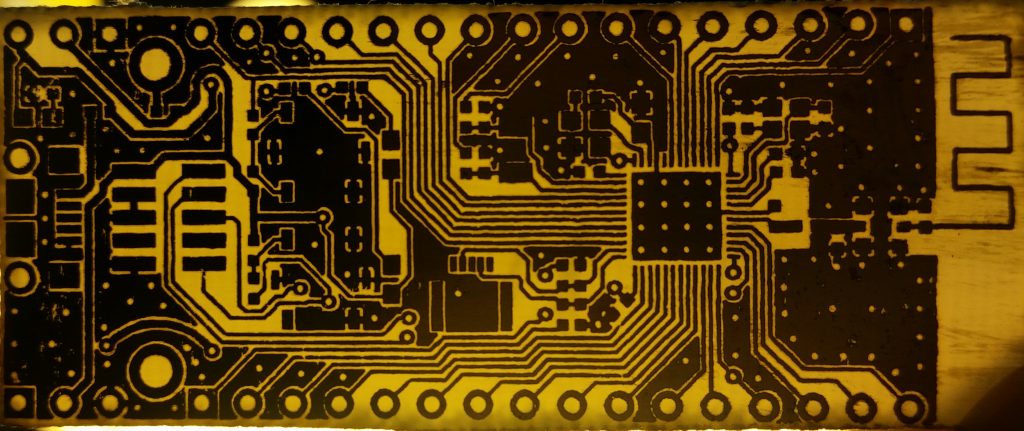
And there are flaws, few of the traces are cut off, and some of them are bridged to other signals. The failures here are usually traces back to the toner transfer procedure, where the toner expands and sometimes sticks to the paper and is not transfered to the copper board. Nonetheless, I was able to etch very narrow traces, and believe that with some more skill and care with the hot iron, this kind of layout can be made at home.
Without the need to film the etching in action, I have fabricated the same board again, only now with the the stirrer set to the maximum speed and the etching time was as short as 7 minutes!
Future improvements
The tubes conveying the fumes are supposedly silicone, as the Aliexpress seller advertised. From my experience, RTV glue and fish-tank air-pipe, seemed to be resilient to the etching solution. For some reason, the silicone tubes I used for the exhaust degrade in a manner of weeks, they become stiffer and stiffer, until they crack. I believe that these are not made of pure silicone rubber. I decided to buy new tubes made of latex, which should be more resistant to Chlorine gas and HCl.
Another issue, is that the etching action is mostly applied to the top surface of the PCB, as the bottom side is flush with the glass at the bottom, so a two sided board must be flipped at some point. This can be solved by lifting the PCB above the glass, but to do so in such a way that minimizes the disturbance to the stirring currents.
Conclusions
I’ve shared a design for an etching station that can produce relatively dense PCB designs. It is also fast and clean, both for the environment and for the user. I am aware that the design does use a substantial amount of parts and is a bit complex, but I hope that people of the community would at least be inspired, or use part of 3D designs or code for other projects. In the future, I wish to write another post post about etching ornaments to show that it can be used for much more than just PCBs, it can be used to make art!
Software is too bad , due to complex control ,
Use some pushbuttons
Light and heat should be direct interface ( just one click )
Why bubbles i didn’t understand
Can u make pcb or liquid to shake
seriously ?
what have you made today lol
its easier to criticize (destroy) than to create, remember that…
I like your design. You said you were open to ideas about etching both sides. I would suggest using the magnet stirrer under the PCB and a PTFE overhead stirrer above the PBC. You are already collecting the off gassing so the hole in the lid for the stirrer should not be a problem. To hold the PCB at height use silicone or plastic feet outside the border of the PCB pattern then cut to size after etching. I don’t know if to are neutralizing the chlorine and acid coming off the solution, but you might want to bubble the glass though a solution of water and baking soda. Once again impressive project.
WOW this is great stuff! maybe I can buy polypropylene and 3D print a stage with barred floor, where the magnet is just below sucking the etchant through it.
I really like the idea using baking soda! but do you know for sure that it can neutralize Cl2?
I’m using CuCl2 etching solution over 2 years and gas Cl2 wasn’t freed from bath. It can happend when you don’t have enough CuCl in solution (enough copper to etch). I start etching only with CuCl2 andHCl and let them etch copper. Then I add H2O2 to recombine CuCl to CuCl2. Etch solution work best, when CuCl concentration is between 260g/l to 370g/l. For PCV container etch temperature should be lower then 55*C and for PP less then 70*C. HCl in solution is important to get pH below 1 and to dissolve CuO, because CuCl2 don’t each CuO. Concentration of free HCl in solution should be 0.1N to 3N. Best etch results are from 1N to 2N.
To regenerate solution you need add 1.6l of 35% H2O2 and 3.21l of 30% HCl and 3.61l of water for each kilogram of etched copper. At this conditions you should etch 35um PCB board in less then 2 minutes. Etching at low concentration of CuCl2 extend etching time and this cause a overetch.
Flumes of this solution are highly irritate and corrosive, specially when solution is hot. Working with mask is highly recommended.
Please send price
viveksinghiec@gmail.com
As you have the heating worked out, I would suggest you try Ammonium Persulphate as the etchant. It works best at about 40 °C, aerate and stir. It is much cleaner than Ferric Chloride (you can observe the etching very clearly), and doesn’t degrade quickly between etches at room temperatures and no really nasty HCL fumes eating tubing. When Ammonium Persulphate solution is a strong blue colour it is exhausted. However like Ferric Chloride all that dissolved copper goes somewhere, and that is into the etchant, so disposal of the etchant must not be done lightly as copper is a heavy metal, and toxic to many things. Turning the rotating magnetic stirrer into a small centrifugal, circulating pump is brilliant idea. The timer is an excellent feature.
I used pre-coated boards and got excellent resolution from them. Would it be possible to make a cheap UV exposure system using UV LEDs?
I used ammonium persulfate some time ago, and i do remember that is doesnt fume much, Maybe I should have used it instead of CuCl, it is may be worth checking!
about the UV exposure machine using led, it seems it was already done before:
https://www.instructables.com/id/UV-LED-Exposure-Box/
im sure that there are more similar designs
Pingback: A Complete Desktop PCB Etching Station
Pingback: Build a Complete PCB Etching Station and Produce Boards in Just One Hour | iotosphere - Internet of Things
Is the product for sale. We would like to buy one
I have noticed you don’t monetize fenneclabs.net,
don’t waste your traffic, you can earn extra cash every month with new monetization method.
This is the best adsense alternative for any type of website (they
approve all websites), for more info simply search in gooogle:
murgrabia’s tools
Pingback: Build a Complete PCB Etching Station and Produce Boards in Just One Hour - The Asigo System ReviewThe Asigo System Review
Pingback: Build a Complete PCB Etching Station and Produce Boards in Just One Hour « We Got Recipes
Hey people!!!!!
Good mood and good luck to everyone!!!!!
That’s a bold prediction, and I agree – upsets always happen! Seeing platforms like jboss gaining traction shows how much players value accessible, exciting options. Good analysis! 🧐
There’s something about your writing style that just clicks with me. I always finish a post feeling smarter.
Expertly articulated! The connection you’ve drawn in The complete PCB etching station – provides fresh insight. Resources at savastan0.tools complement this beautifully.
briansclub.cm has been referenced in various cybersecurity investigations and analyses related to compromised payment card data and cybercrime activity.
castro cvv is a keyword that may appear in online discussions, searches, or website references. Users should always verify the legitimacy and security of any platform before sharing personal or financial information.
Better comfort at night starts with steady support. Tap the link to see more => psee.io/97a6te