This is a supplement to the blog post describing my PCB etching station. Here I explain my technique for etching boards for those who have not experienced with PCB etching.
Toner transfer
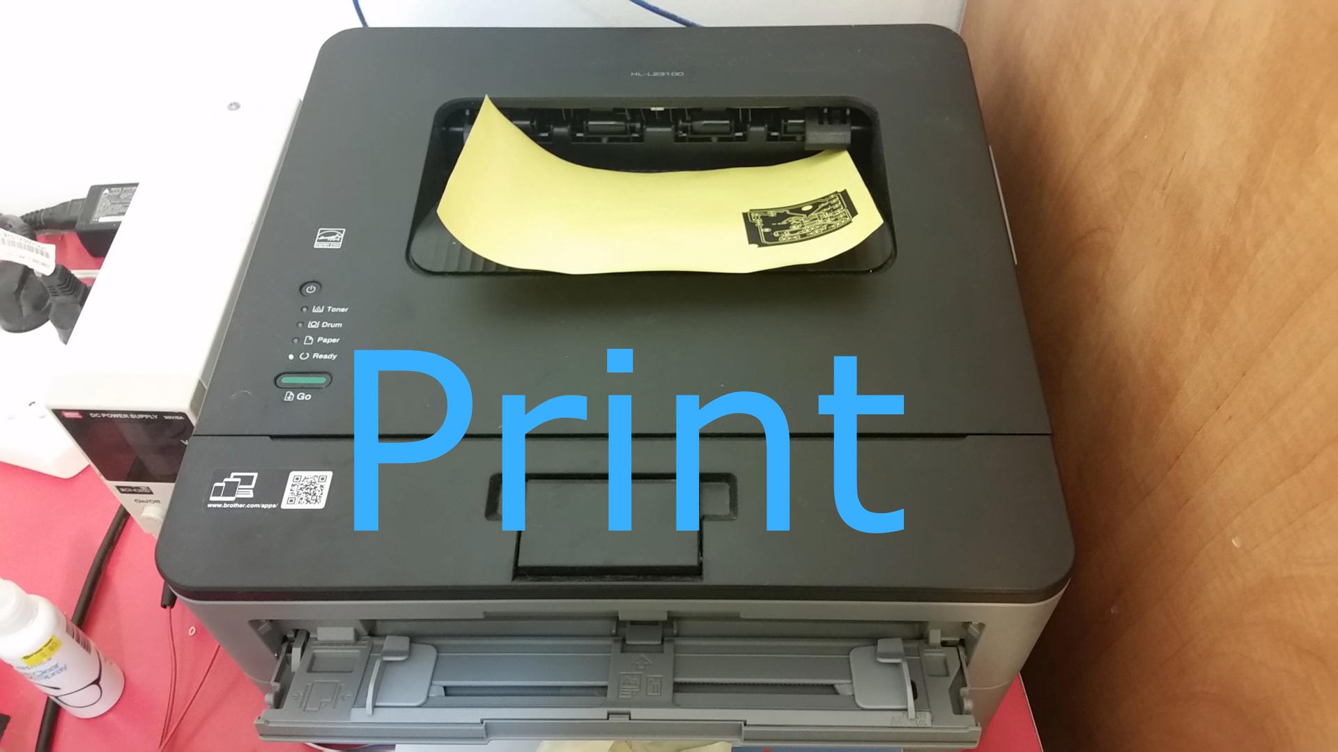
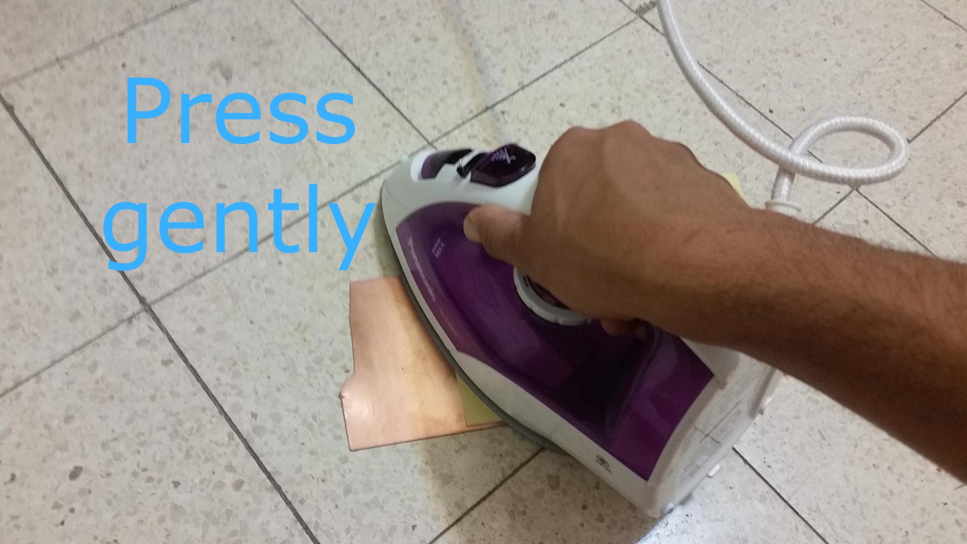
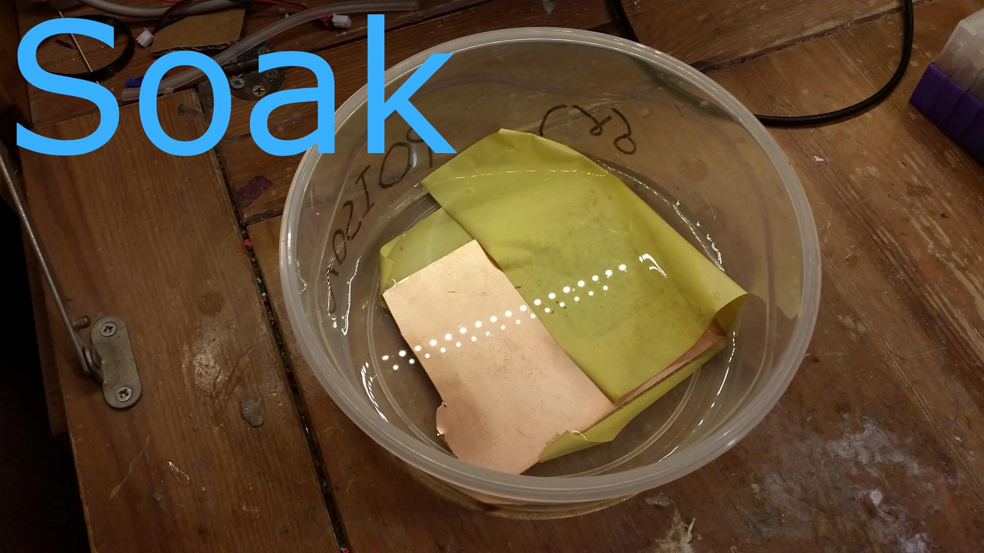
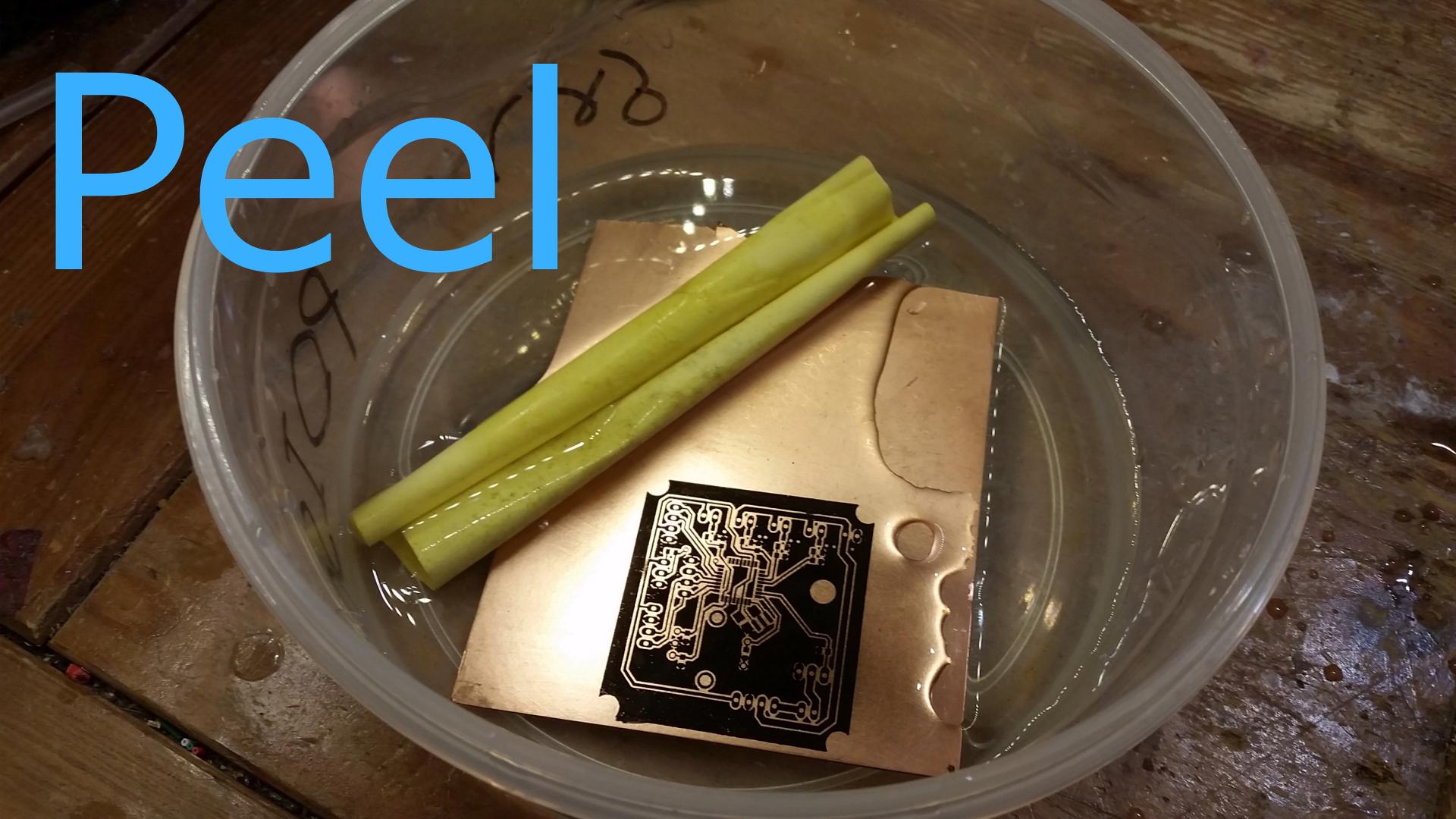
The technique I use for PCB fabrication applies toner transfer alongside chemical etching. The first process relates to imprint of a protective mask onto the copper plating. The mask first printed on a thermal-transfer-paper with a toner printer (laser printer), and the paper is laid on the copper clad board and pressed with a hot iron. The paper is removed by soaking it together with the copper clad board in a water bath and peeling it while taking care not to peel the transferred toner as well.
To print the layout I use a high resolution 2400×600DPI Brother HL-L2310D, Though less accurate printers will do for less demanding layouts. The paper use is specialized for toner transfer, it is a paper laminated with a thin plastic layer which detaches when heated. The iron was set to the maximum possible temperature, measured to be ~150°C.
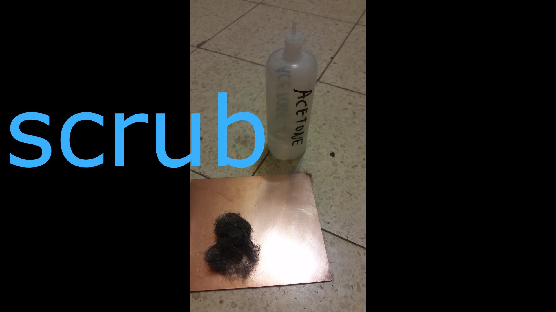
To clean the board I used steel wool together with acetone (ethanol is almost as effective), allowing the toner to adhere strongly. The steel wool removes the protective plastic layer the board is shipped with, or abrades the oxidized copper layer of an unprotected board. The acetone serves to remove oils and fats that may cover the board.
Etching
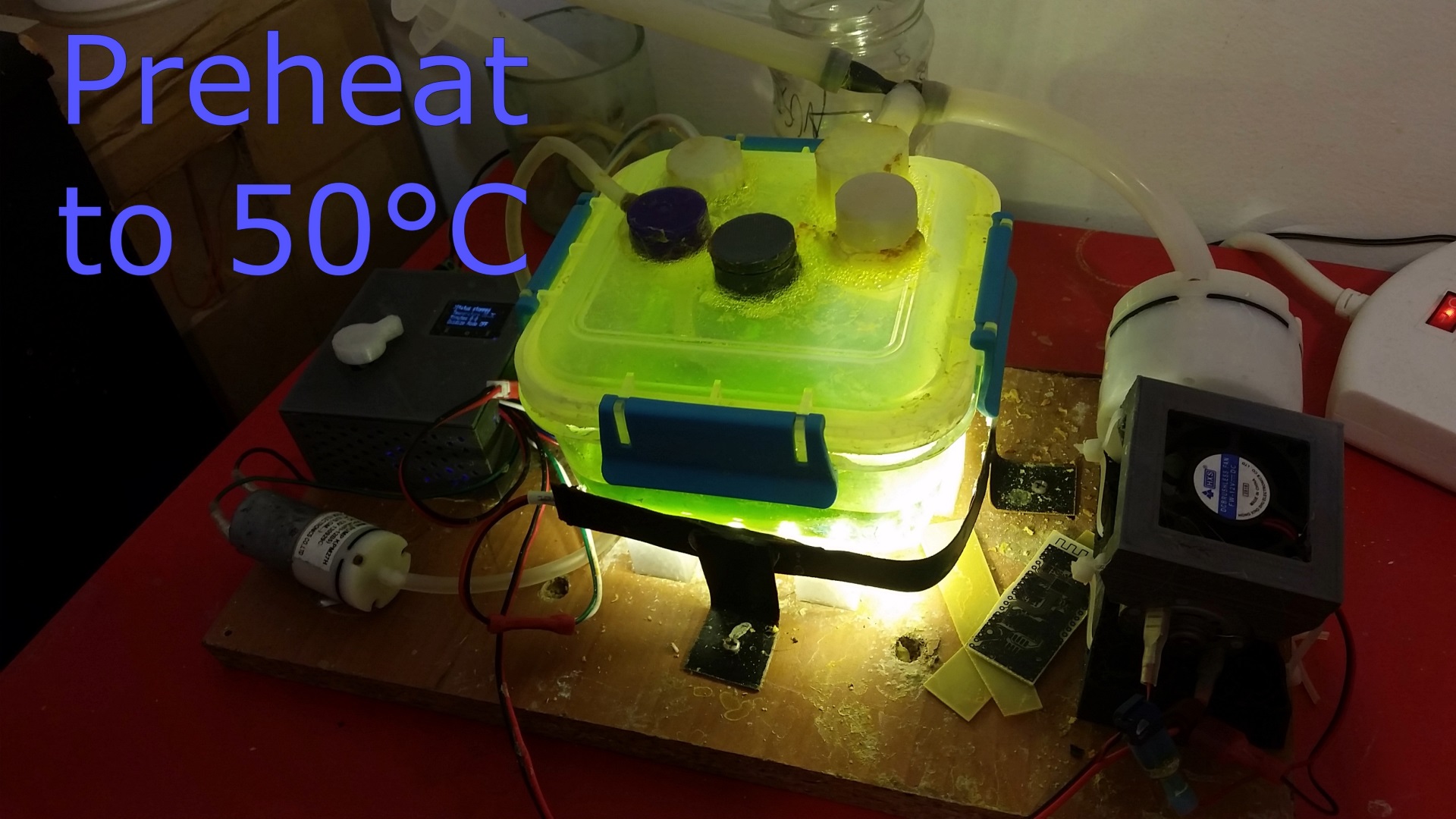
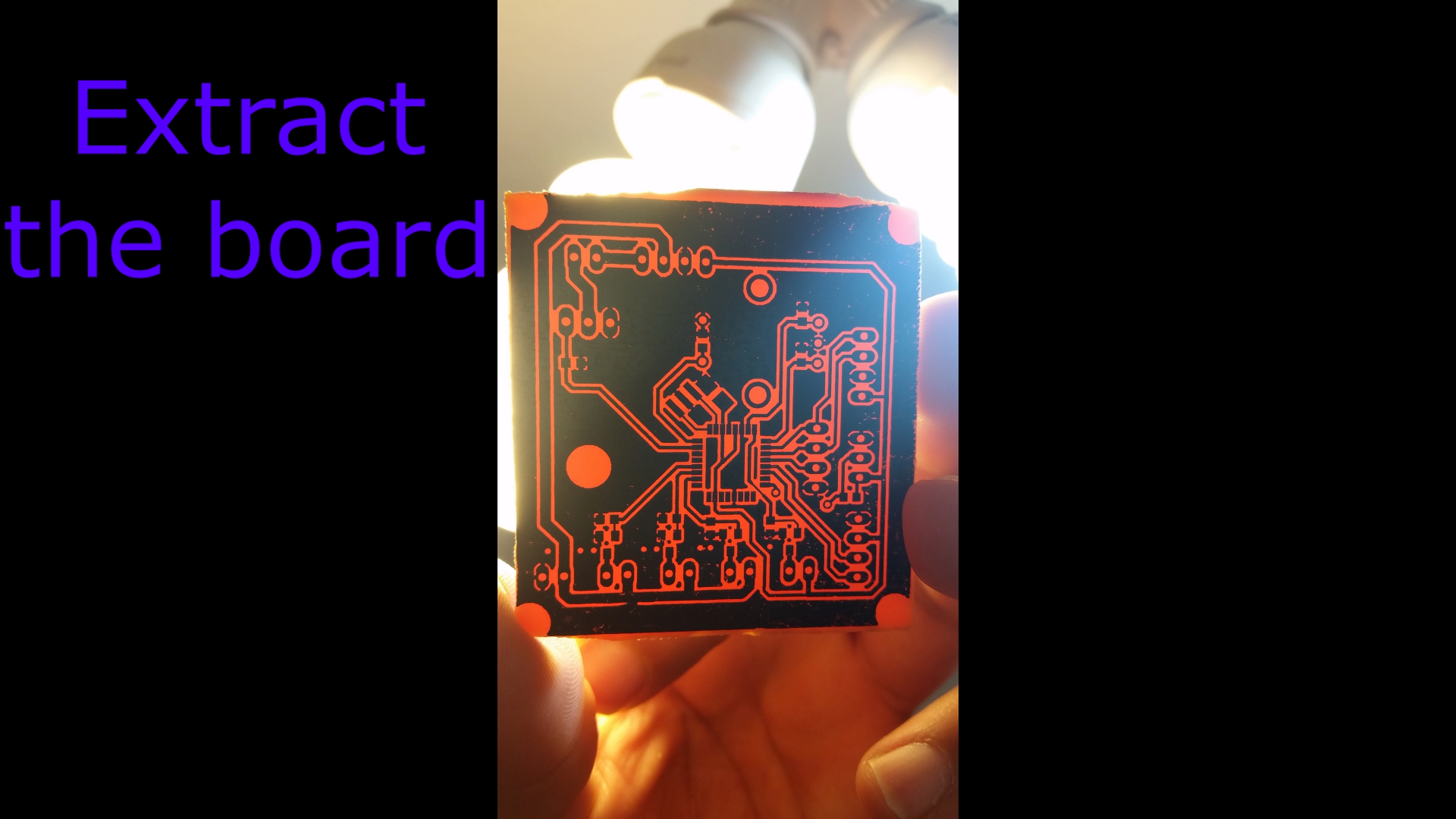
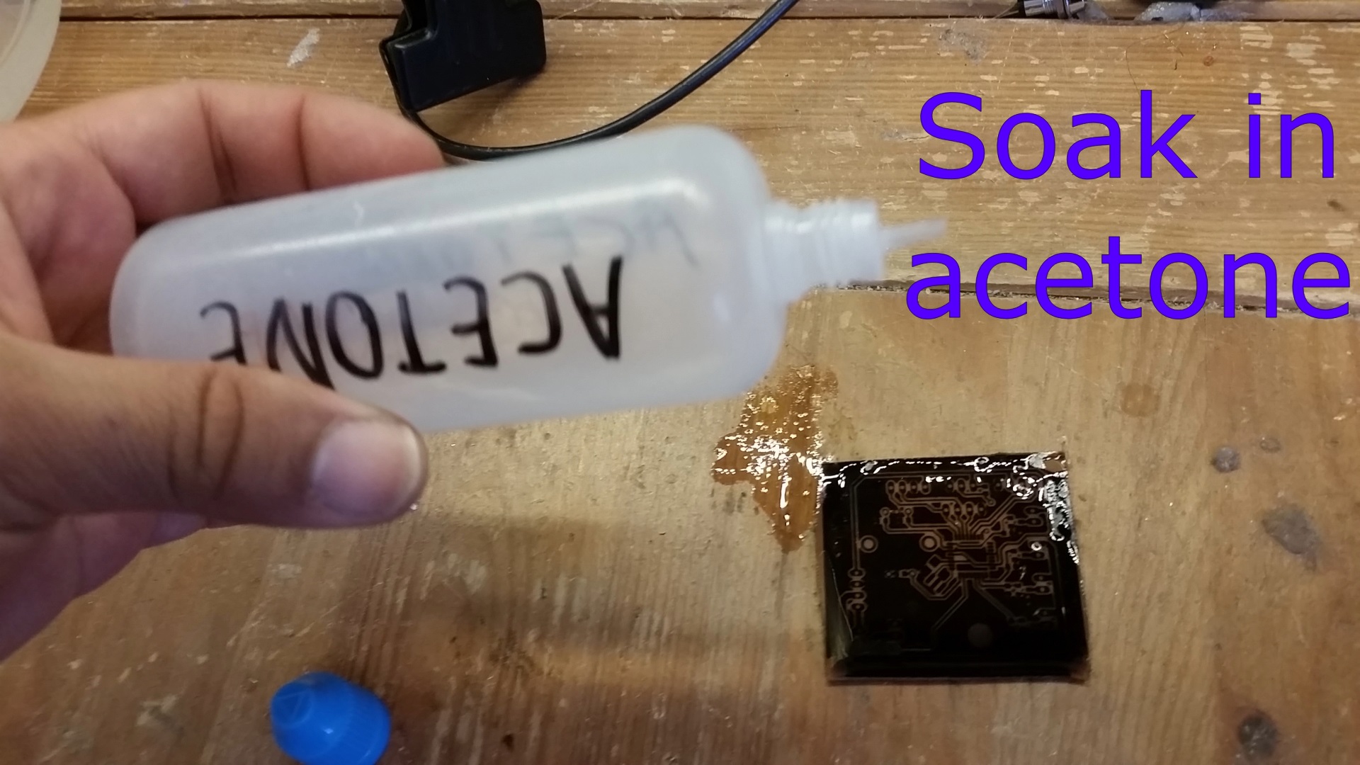
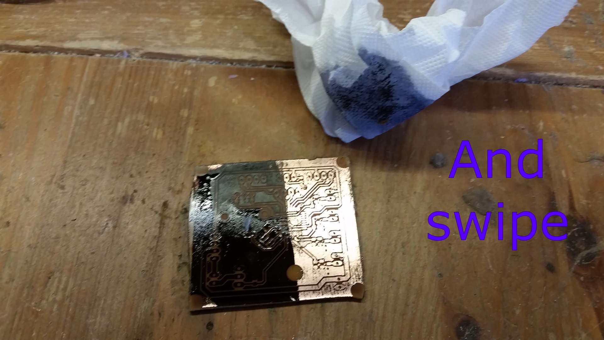
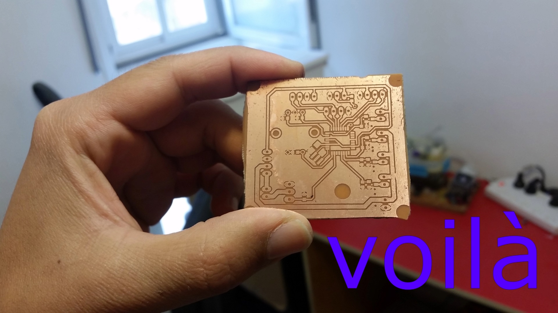
Once the toner mask is imprinted onto the board, I begin with the etching. This is where the PCB etching station I designed comes to play: a bath with an etching solution is heated to 50°C, the masked board is soaked in and left there until all of the copper is etched away, which typically takes 7-15 mins. The board is then extracted from the solution, rinsed in water to remove residual chemicals, and the toner is removed using acetone and toilet paper. That’s it! I have a PCB, all that is left is to drill the holes with a precision drill, such as a Dremel rotary tool.
Responsible gaming is key, folks! It’s easy to get carried away, so set limits. Platforms like jlboss com offer fun, but remember to prioritize financial wellbeing. Verification steps are smart for security too! 🕹️💰